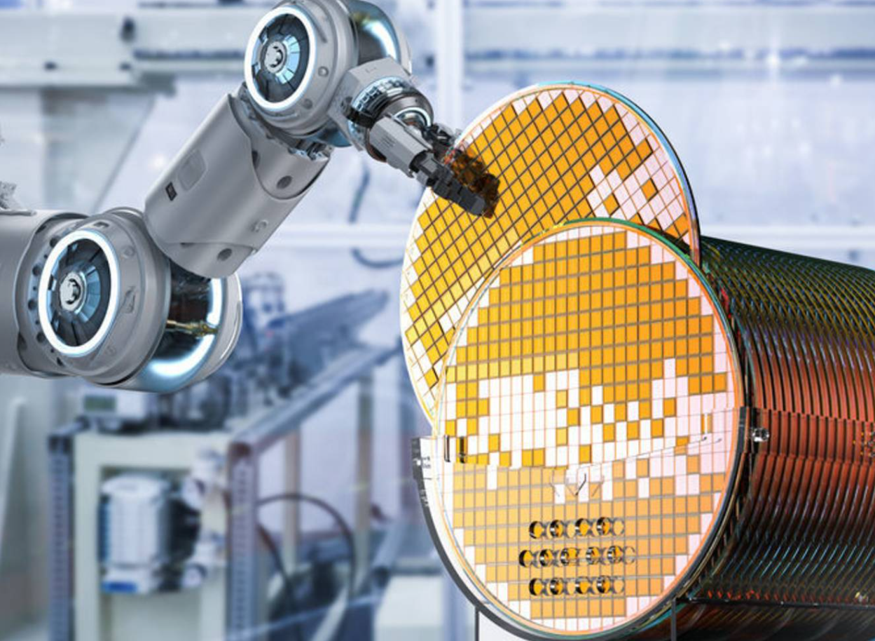
A semiconductor equipment supplier is a professional company that provides the machines and technologies required for wafer fabrication, packaging & testing, and process automation.
These systems cover the entire process chain — from front-end wafer processing (such as lithography, etching, ion implantation, and thin-film deposition) to back-end packaging (such as dicing, bonding, inspection, and CNC precision machining fixtures).
Their main roles include:
🔧 Providing high-precision process equipment (e.g., CVD/PVD systems, CNC machining tools, laser dicing, vacuum systems)
🧠 Supporting process integration and automation (e.g., robotic handling, control systems, data monitoring)
📈 Helping semiconductor manufacturers improve yield and production efficiency
In short, semiconductor equipment suppliers are the key bridge connecting materials, processes, and manufacturing, and are a driving force behind the continuous advancement of semiconductor technology.
front stage
Four major core manufacturing processes for semiconductor bodies
Photolithography
Photolithography is the process of transferring circuit patterns onto a wafer using light. Photoresist coating, exposure, and development define the areas for subsequent etching or deposition.
蝕刻(Etching)
Etching removes unwanted material from the wafer according to the photolithography pattern. It can be wet (chemical) or dry (plasma), with dry etching offering high precision and vertical profile control.
離子佈植(Ion Implantation)
Ion implantation introduces dopant elements (such as boron, phosphorus, or arsenic) into silicon using a high-energy ion beam, modifying its electrical properties to form P-type or N-type regions.
薄膜沉積(Thin Film Deposition)
Thin film deposition forms conductive, insulating, or semiconductor layers on a wafer. Common methods include Physical Vapor Deposition (PVD), Chemical Vapor Deposition (CVD), and Atomic Layer Deposition (ALD).
Back-End
Dicing
Dicing is the process of precisely cutting a semiconductor wafer into individual dies. Diamond blade sawing and laser dicing are commonly used, with strict control of depth and speed to prevent chipping or cracking.
Bonding
Bonding connects the chip to a substrate or lead frame, forming both electrical and mechanical connections. Common types include wire bonding, flip-chip bonding, and wafer-level bonding.
Testing
Testing and inspection ensure chip functionality and quality after packaging. It includes electrical testing, visual inspection, and X-ray or AOI inspection to verify interconnections and package integrity.
CNC precision
CNC precision machining fixtures are used to hold and position chips or modules during packaging and testing, ensuring process stability and accuracy. They are typically made of aluminum, stainless steel, or engineering plastics with high rigidity and precision.
Yongyi Technology Co., Ltd.
location_on 42756 No. 188-9, Section 1, Dafeng Road, Tanzi District, Taichung City, Taiwan
email yongyi-sales@umail.hinet.net
email justinwu6767@gmail.com