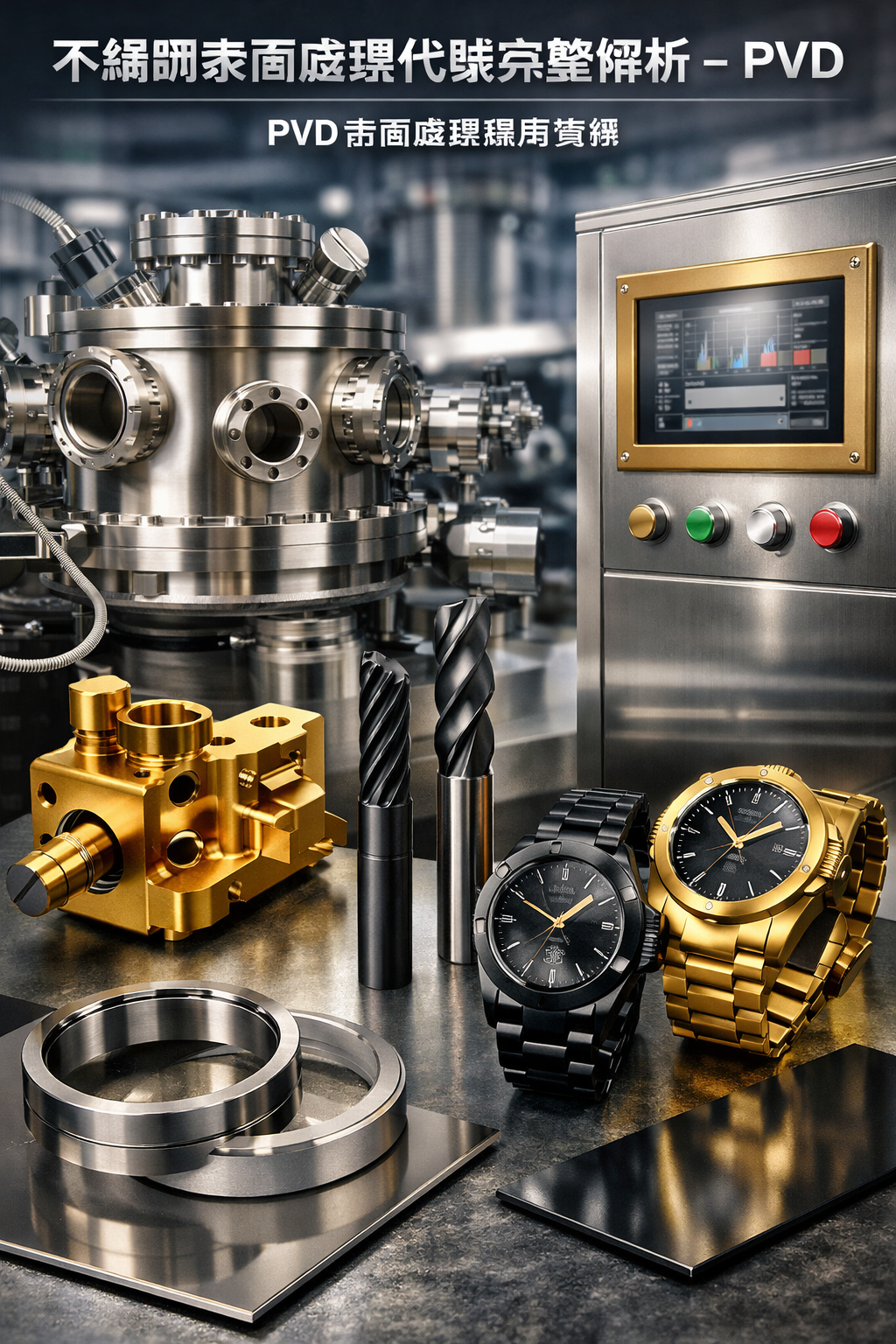
Complete Explanation of Stainless Steel Surface Treatment Codes: PVD (Physical Vapor Deposition) x Suitable for semiconductor equipment, CNC precision components, industrial appearance parts, and high-end equipment manufacturing x Processing method – vacuum coating
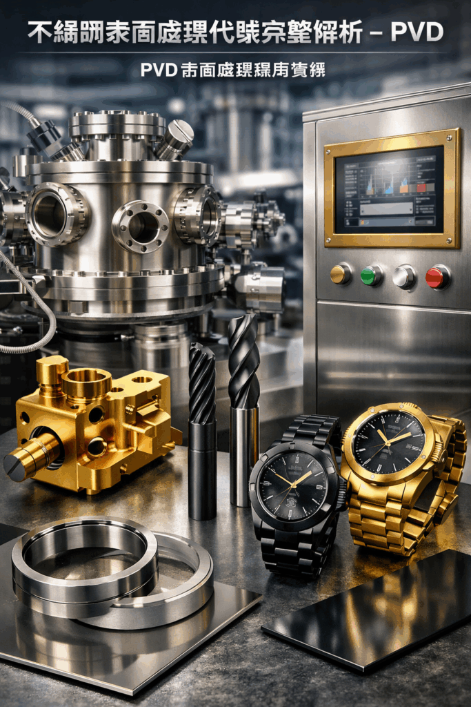
Complete Guide to Stainless Steel Surface Finish Codes — PVD
1. What is PVD? (Nature of the Surface Treatment)
PVD (Physical Vapor Deposition) is a vacuum coating technology in which metallic or ceramic materials are vaporized (by evaporation or sputtering) in a vacuum environment and deposited onto the surface of a stainless steel substrate, forming a high-adhesion, ultra-thin, high-performance functional coating layer.
📌 PVD is a coating, not electroplating and not painting
📌 The coating thickness is extremely thin (approx. 1–5 μm), with negligible impact on dimensional accuracy
2. What Materials Are Used in PVD?
1️⃣ Substrate Materials
PVD can be applied to most stainless steel grades:
| Stainless Steel Grade | Characteristics |
|---|---|
| SUS304 | General-purpose, good corrosion resistance |
| SUS316 / 316L | Excellent corrosion resistance (semiconductor / medical use) |
| SUS420 / 440 | Hardenable, high strength |
| SUS303 | Free-machining (adhesion requires special attention) |
2️⃣ PVD Coating Materials (Functional Layers)
| PVD Code | Coating Material | Color | Main Characteristics |
|---|---|---|---|
| TiN | Titanium Nitride | Gold | High hardness, wear resistance |
| CrN | Chromium Nitride | Silver-gray | Corrosion resistance, low friction |
| ZrN | Zirconium Nitride | Champagne gold | Decorative + corrosion resistance |
| TiCN | Titanium Carbonitride | Dark gray | Extreme wear resistance |
| DLC | Diamond-Like Carbon | Black | Ultra-low friction |
| AlTiN | Aluminum Titanium Nitride | Dark black-violet | High-temperature stability |
📌 Common for semiconductor equipment: CrN / TiN / DLC
📌 Common for decorative and equipment enclosures: TiN / ZrN
3. PVD Process Flow (Industrial Standard)
🔧 Stainless Steel PVD Process Steps
CNC machining completed
↓
Surface pre-treatment (Grinding / Polishing / HL / Matte)
↓
Ultrasonic cleaning (degreasing & particle removal)
↓
Loading into vacuum chamber
↓
Vacuum pumping (10⁻³ – 10⁻⁶ Torr)
↓
Ion cleaning (Ar plasma)
↓
PVD coating deposition (Arc / Sputtering)
↓
Cooling → Unloading → Final inspection
📌 Surface pre-treatment quality is the key success factor for PVD
📌 Surface defects will be fully replicated after coating
2️⃣ Common PVD Technologies
| Process Type | Features | Applications |
|---|---|---|
| Arc Ion Plating | High adhesion | Industrial wear-resistant parts |
| Magnetron Sputtering | Uniform coating | Precision equipment |
| Multi-layer PVD | Layered structure | Advanced semiconductor applications |
4. PVD Surface Properties (Engineering Data)
| Item | PVD Performance |
|---|---|
| Coating thickness | Approx. 1–5 μm |
| Hardness | HV 1800–3500 |
| Adhesion | Extremely high (no peeling) |
| Friction coefficient | 0.1–0.4 |
| Temperature resistance | Approx. 400–800°C (material dependent) |
| Dimensional impact | Negligible |
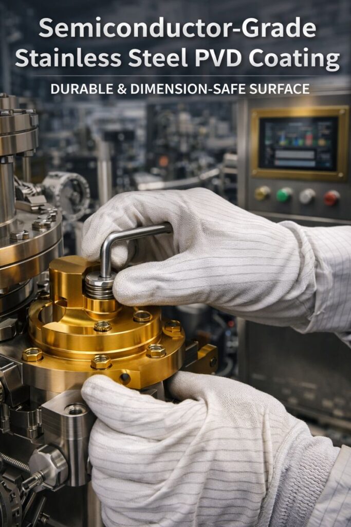
5. Applications of PVD on Stainless Steel
🔹 1️⃣ Functional Applications (Industrial / Semiconductor)
| Component | Purpose |
|---|---|
| Vacuum chamber components | Particle resistance, corrosion resistance |
| Semiconductor mechanical parts | Wear resistance, anti-sticking |
| Automated sliding parts | Low friction |
| CNC tool holders | Extended service life |
🔹 2️⃣ Aesthetic & Identification Applications
| Item | Effect |
|---|---|
| Equipment enclosures | Premium metallic appearance |
| Brand identification parts | Colorfast, non-fading |
| Control panels | Fingerprint resistance |
🔹 3️⃣ Combination with Other Surface Finishes
| Pre-treatment | Effect with PVD |
|---|---|
| HL (Hair Line) | High-end industrial appearance |
| Mirror polishing | Mirror-like metallic finish |
| Bead blasting | Uniform matte surface |
6. What Does the Final PVD Product Look Like?
📦 Characteristics of PVD Stainless Steel Products
- Uniform surface color, no discoloration
- Retains original stainless steel texture (HL / polished)
- High hardness, scratch-resistant
- No impact on assembly tolerances
- Suitable for long-term use in vacuum and chemical environments
📌 PVD is a premium surface treatment combining functionality and aesthetics
7. Comparison: PVD vs Other Surface Treatments
| Item | PVD | Electroplating | Painting |
|---|---|---|---|
| Coating thickness | Ultra-thin | Thick | Thick |
| Dimensional impact | Minimal | Noticeable | Significant |
| Wear resistance | Excellent | Moderate | Poor |
| Vacuum compatible | ✅ | ❌ | ❌ |
| Semiconductor suitable | ✅ | ❌ | ❌ |
8. Engineering & Purchasing Notes (Important)
✔ SUS303 requires special treatment to ensure adhesion
✔ Not suitable for deep holes or shielded areas requiring uniform thickness
✔ Higher cost than electroplating, but significantly longer service life
✔ Suitable as a standard process for exporting equipment to Europe (Germany / Switzerland)
✅ One-Sentence Summary
PVD is a key surface treatment technology for stainless steel in high-end equipment and semiconductor industries, balancing functionality, durability, and appearance.
🔹 Hashtags
#PVDcoating #PhysicalVaporDeposition #SemiconductorGradePVD #VacuumCompatibleCoating #LowParticleGeneration #DimensionSafeCoating #ThinFilmCoating #StainlessSteelPVD #SUS304PVD #SUS316LPVD #PrecisionStainlessSteel #PVDCoatedStainlessSteel #TiNCoating #CrNCoating #ZrNCoating #DLCCoating #AlTiNCoating #MultiLayerPVD #SemiconductorEquipmentComponents #VacuumChamberParts #WaferHandlingComponents #CleanroomCompatible #LowOutgassing #ArcIonPlating #MagnetronSputtering #WearResistantCoating #HighHardnessCoating #LowFrictionSurface #CoatingThickness1to5um #ISO26443 #LotTraceability #SemiconductorOEM #PVDCoatingSupplier #CNCMachiningAndPVD
🔹 Deutsch – Deutschland
#PVDBeschichtung #EdelstahlBeschichtung #HalbleiterEquipment #VakuumkompatibleBeschichtung #PartikelarmeOberfläche #HochpräziseBauteile #VerschleißfesteBeschichtung #MaßhaltigeDünnschicht #Edelstahlteile #Halbleiteranlagen
🔹 Deutsch – Schweiz
#HochpräzisePVDBeschichtung #EdelstahlteileHalbleiter #Reinraumtauglich #NiedrigeAusgasung #Präzisionsbeschichtung #Vakuumanwendungen
#SemiconductorGradePVD #StainlessSteelPVD #VacuumCompatible #LowParticle #PrecisionComponents #Halbleiteranlagen #PVDBeschichtungEdelstahl #SemiconductorEquipment
Yongyi Technology Co., Ltd.

location_on 42756 No. 188-9, Section 1, Dafeng Road, Tanzi District, Taichung City, Taiwan
email yongyi-sales@umail.hinet.net
email justinwu6767@gmail.com