🧩 Introduction and Applications of Key Components and Materials for Semiconductor Equipment
- Semiconductor Materials
First-generation semiconductors: Primarily silicon, they are the most widely used material in commercial applications.
Second-generation semiconductors: Gallium arsenide (GaAs) and indium phosphide (InP) are representative, primarily used in high-frequency communication products.
Third-generation semiconductors: Primarily silicon carbide (SiC) and gallium nitride (GaN), they are used in high-power applications such as electric vehicles and base stations. 2. Key Component Materials
Material Types: Includes aluminum, stainless steel, brass, titanium alloys, ceramics (such as alumina, zirconia, and silicon nitride), quartz, engineering plastics, and composite materials.
Ceramic Materials:
Alumina: Low cost, suitable for structural components in medium-temperature zones.
Zirconium Oxide: High toughness and strength, suitable for moving parts or components that dynamically interact with mechanisms.
Silicon Nitride: High thermal shock resistance, suitable for high-temperature or rapid cooling and heating processes.
Component Examples: Vacuum chamber components such as shower heads, clamp rings, and chamber lids. - Process Chemicals and Consumables
Chemicals and Photoresists: Used in semiconductor manufacturing processes. For example, photoresists are used in photolithography, while high-purity chemicals are widely used in etching and cleaning.
Silicon Wafers: Serves as the substrate material for semiconductor products.
Others: Such as sealing materials and lubricants used in equipment. 4. Process Technology
Precision Machining and Surface Treatment: Ensures that parts meet stringent dimensional and tolerance requirements.
Vacuum Processing: Techniques such as etching, chemical vapor deposition (CVD), and physical vapor deposition (PVD) require highly precise and clean equipment and components.
Ion Implantation: Used to modify material properties, particularly in ceramic applications to improve durability.
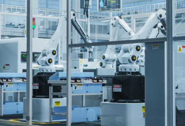
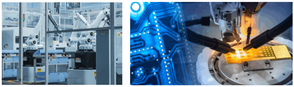
Key components and materials for semiconductor equipment include semiconductor materials, high-end components, and chemicals and consumables used in the equipment. Semiconductor materials such as silicon, gallium arsenide, and silicon carbide are the foundation of wafer manufacturing. Key components include critical parts within the vacuum chamber, such as the showerhead and retainer ring. These parts require high-precision machining and are often made of materials such as aluminum, stainless steel, and ceramic. In addition, consumables such as chemicals, photoresists, and silicon wafers are used in the manufacturing process.
Semiconductor manufacturing is an extremely precise and clean process. From silicon wafer materials and process chemicals to key components, purity, stability, and reliability must be strictly controlled. For equipment suppliers, these materials and components are not only the core of process stability but also crucial for improving production capacity and yield.
For the metal, ceramic, transparent, and elastic sealing materials listed in “Introduction to Materials for Key Semiconductor Equipment Components,” this section explains their primary uses, characteristics, and application areas.
Semiconductor Equipment Key Component Material Introduction and Applications
🔹 1. Metal Materials
| Material | Main Properties | Semiconductor Applications |
|---|---|---|
| Aluminum Alloy | Lightweight, high thermal conductivity, corrosion-resistant, easy to machine | Used for vacuum chambers, equipment frames, support structures, and CVD/PVD chamber parts. Anodized for better corrosion resistance and insulation. |
| Titanium (Ti) | High strength, low density, corrosion and chemical resistance | Used in vacuum chamber structures, gas fittings, thin film targets, and structural bolts; ideal for corrosive gas environments. |
| Tungsten (W) | High melting point, high density, excellent electrical and thermal conductivity | Applied in etching electrodes, heaters, and PVD/CVD targets for high-temperature environments. |
| Copper (Cu) | Excellent electrical and thermal conductivity, easy to machine | Used for electrodes, conductors, and heat dissipation modules (e.g., heater chuck, cold plate); surface treated to prevent oxidation. |
| Tantalum (Ta) | Corrosion-resistant, high melting point, good conductivity | Commonly used for etching electrodes, PVD targets, and diffusion barrier layers. |
| Molybdenum (Mo) | High strength, temperature stability, good conductivity | Used in PVD targets, reflectors, electrodes, and high-temperature platforms. |
🔹 2. Ceramic Materials
| Material | Main Properties | Semiconductor Applications |
|---|---|---|
| Alumina (Al₂O₃) | High hardness, insulation, wear resistance | Used in insulating rings, electrode supports, chamber spacers, and CMP polishing bases. |
| Aluminum Nitride (AlN) | High thermal conductivity, excellent insulation, low expansion | Used in heater chucks, thermal modules, and laser bases requiring fast heat transfer. |
| Silicon Carbide (SiC) | High hardness, corrosion resistance, plasma durability | Applied to etching chambers, liners, shields, and electrostatic chucks. |
| Silicon Nitride (Si₃N₄) | High toughness, strength, and thermal shock resistance | Used for support rings, vacuum insulators, bearings, and sealing rings. |
🔹 3. Transparent Materials
| Material | Main Properties | Semiconductor Applications |
|---|---|---|
| Quartz (SiO₂) | High purity, transparency, thermal shock resistance | Used for lithography windows, CVD tubes, shields, and UV/EUV optics. |
| Glass | Cost-effective, insulating, design-flexible | Used for observation windows, control panels, optical interfaces, and test jigs. |
| Sapphire (Al₂O₃ Single Crystal) | High hardness, transparency, heat resistance | Used as EPI substrates, laser windows, and optical sensor lenses. |
🔹 4. Elastic and Sealing Materials
| Material | Main Properties | Semiconductor Applications |
|---|---|---|
| Fluoroelastomer (FKM) | Heat and chemical resistant, excellent gas tightness | Used for vacuum O-rings, valve seals, and chemical gas line sealing. |
| O-Ring | High elasticity, reliable sealing | Used in flanges, valves, and cooling modules (materials: FKM, EPDM, or FFKM). |
| Vacuum Seal Components | High vacuum resistance, low outgassing | Used in gate valves, load locks, and chamber interfaces. |
🧠 Summary
- Metals → Structure, conductivity, and thermal management.
- Ceramics → Insulation and plasma corrosion protection.
- Transparents → Optical precision and process observation.
- Elastomers → Vacuum sealing and chemical resistance.
#Semiconductor Materials #Key Components #Silicon Wafers #SiC #GaN #Vacuum Chamber #Photoresist #Process Gases #CMP Slurry #Semiconductor Equipment Supplier #Precision CNC Machining #High-Purity Materials #Clean Process
Semiconductor Equipment #Key Components #Semiconductor Materials #CNC Machining #Vacuum Chamber #Quartz Parts #Ceramic Parts #SiC #Semiconductor Supply Chain #Smart Manufacturing #Wafer Processing #Packaging and Testing #ESG Manufacturing #Automation Integration #PVD #CVD #Etching #CMP #WaferFab #EquipmentSupplier
Yong Yi Technology Co., Ltd.
Yong Yi Technology Co., Ltd. logo
location_on No. 188-9, Section 1, Dafeng Road, Tanzi District, Taichung City, Taiwan 42756
Call +886-4-25341382
ring_volume
+886-4-25341847
Email yongyi-sales@umail.hinet.net
Email justinwu6767@gmail.com