PVD and CVD are two major thin film deposition technologies. Their roles, applications, factory processes, and differences in CNC machining, precision parts manufacturing, semiconductor equipment components, tool coating, and advanced surface engineering are discussed.
PVD (Physical Vapor Deposition) and CVD (Chemical Vapor Deposition) are two major thin film deposition technologies.
PVD relies on physical processes (such as evaporation and sputtering) to vaporize and deposit materials, making it suitable for metal coatings and high-hardness, wear-resistant coatings, and it operates at lower temperatures.
CVD relies on chemical reactions (such as decomposition and synthesis) to form thin films on substrates, offering good coverage and suitability for complex structures. It is commonly used for semiconductor insulating layers and high-quality hard coatings, and typically operates at higher temperatures. PVD (Physical Vapor Deposition) principle: In a high vacuum environment, physical methods (such as heating evaporation and ion sputtering) are used to atomize the material source (target), which is then deposited onto the workpiece surface.
Advantages: Environmentally friendly (no toxic gases), lower film formation temperature (minimal impact on the substrate), good coating adhesion, high hardness, and stable film. Disadvantages: Poor coating properties (3D structure surface is less uniform), difficult deposition at locations opposite the evaporation source. Applications: Wear-resistant coatings for mechanical tools (TiN, TiAlN), decorative coatings (watches, jewelry), semiconductor metal wiring.
CVD (Chemical Vapor Deposition) – Principle: A gaseous precursor containing the deposition material is introduced into a reaction chamber, where it undergoes a chemical reaction or decomposition on the substrate surface to deposit a solid thin film. Advantages: Excellent coating properties (can achieve omnidirectional coverage), high purity and density of the deposited layer, capable of producing complex and thin films. Disadvantages: High reaction temperature (usually above 400°C), often involves harmful gases.
Applications: Semiconductor epitaxy, dielectric layers (SiO₂), conductive metal layers, artificial diamond manufacturing. Overview of Key Differences Between PVD and CVD Characteristics PVD (Physical Vapor Deposition) CVD (Chemical Vapor Deposition) Deposition Mechanism Physical Evaporation/Sputtering Chemical Reaction/Decomposition Reaction Temperature Low (approx. 200°C to 500°C) High (typically >500°C) Poor Coverage (poor field of view, poor for complex 3D structures) Excellent (good conformability, suitable for complex shapes) Extremely High Film Hardness (suitable for hard coatings) High (depends on material) Main Applications Tool surface treatment, metal films, semiconductors, insulating layers, diamond films Summary: How to Choose? Choose PVD: Surfaces requiring low-temperature processing, high hardness, and relatively simple shapes (e.g., milling cutters, drill bits, decorative items). Choose CVD: Thin films requiring fine, high conformability, and high density (e.g., IC transistor structures, complex mechanical parts).
1. What is PVD? (Physical Vapor Deposition)
Physical Vapor Deposition
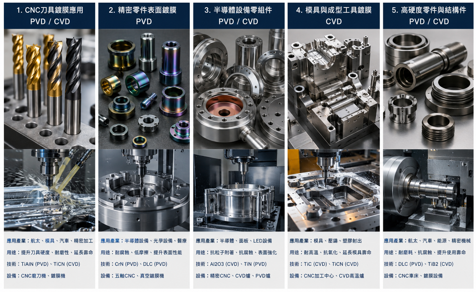
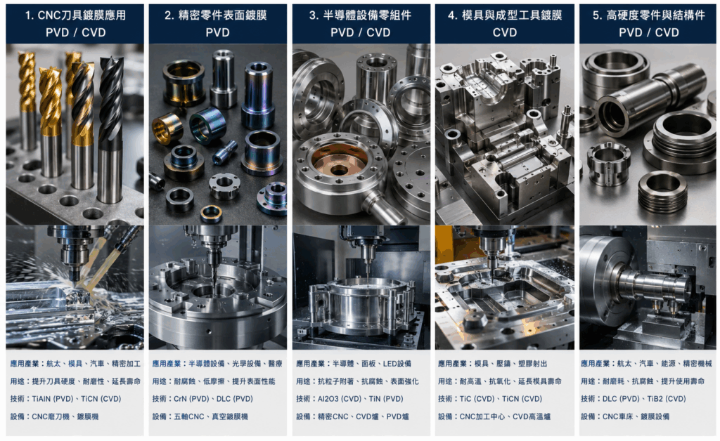
1️⃣ The Role of PVD in CNC Machining
In CNC precision machining, PVD is one of the most widely used technologies for cutting tool coating and precision component surface enhancement. It deposits nanometer-scale thin films onto workpiece surfaces by evaporating or sputtering metallic materials in a vacuum environment.
For applications such as:
- CNC Turning
- CNC Milling
- 5-Axis CNC Machining
- Micro Precision Machining
- High-Speed CNC Cutting
PVD significantly improves:
Key Benefits in CNC Machining:
✅ Increased cutting tool hardness
✅ Reduced cutting friction coefficient
✅ Extended CNC tool life
✅ Enhanced high-speed machining stability
✅ Improved surface roughness quality
✅ Reduced tool chipping rate
✅ Better production consistency in mass manufacturing
PVD has become a standard process especially in:
- CNC Stainless Steel Machining
- CNC Titanium Machining
- CNC Aerospace Components
- CNC Semiconductor Equipment Parts
- CNC Micro Precision Components
2. Applications of PVD in CNC Machining
1️⃣ CNC Cutting Tool Coating
Common PVD coatings include:
- Titanium Nitride (TiN)
- Titanium Aluminum Nitride (TiAlN)
- Chromium Nitride (CrN)
- Diamond-Like Carbon (DLC)
Applied to:
- CNC End Mills
- CNC Drill Bits
- CNC Taps
- CNC Turning Tools
- Micro Machining Tools
These coatings ensure long-term stable cutting performance for CNC machining, 5-axis machining, and automated manufacturing lines.
2️⃣ Precision CNC Component Coating
Applications include:
- Semiconductor Vacuum Chamber Components
- Precision Fixtures
- Linear Guide Components
- Bearing Housings
- Optical Equipment Parts
Benefits:
✅ Wear Resistance
✅ Scratch Resistance
✅ Corrosion Resistance
✅ Low Friction
✅ Dimensional Stability
This is especially critical for:
- High-Precision CNC Parts
- OEM Precision Components
- Semiconductor Equipment Manufacturing
3. PVD Factory Process (CNC Manufacturing Workflow)
Step 1: CNC Precision Machining
- CNC Milling
- CNC Turning
- 5-Axis Machining
- Precision Grinding
Ensuring tight dimensional tolerances.
Step 2: Surface Pre-Treatment
- Ultrasonic Cleaning
- Degreasing
- Acid Cleaning
- Plasma Cleaning
Ensuring contamination-free CNC surfaces.
Step 3: Vacuum Coating
Inside vacuum chambers:
- Evaporation
- Arc Ion Plating
- Magnetron Sputtering
Depositing thin films onto CNC machined parts.
Step 4: Quality Inspection
- Coating Thickness Measurement
- Adhesion Testing
- Surface Roughness Inspection
- CNC Dimensional Verification
Ensuring precision machining quality.
4. What is CVD? (Chemical Vapor Deposition)
Chemical Vapor Deposition
CVD is a coating technology that forms thin films through high-temperature chemical reactions of gaseous precursors on the workpiece surface.
It plays a critical role in:
- CNC Precision Machining
- Hard Cutting Tool Manufacturing
- Semiconductor Equipment Components
- High-Temperature Wear-Resistant Parts
5. The Role of CVD in CNC Machining
CVD is especially effective for high-load CNC cutting applications.
Key Benefits in CNC Machining:
✅ Ultra-high hardness
✅ High-temperature oxidation resistance
✅ Stable high-speed cutting performance
✅ Superior wear resistance for heavy cutting
✅ Extended cutting tool life
✅ Ideal for long-hour automated CNC production
Best suited for:
- Cast Iron CNC Machining
- Alloy Steel CNC Machining
- Mold Steel CNC Machining
- High-Volume Automated Production
6. Applications of CVD in CNC Machining
Common CVD coatings include:
- Titanium Carbide
- Titanium Carbonitride
- Aluminum Oxide
Applied to:
- CNC Carbide Inserts
- Swiss-Type Lathe Inserts
- Heavy Cutting Tools
- High-Productivity CNC Tooling
7. CVD Factory Process (CNC Manufacturing Workflow)
Step 1: Tool Substrate Manufacturing
- Powder Metallurgy
- Precision Tool Grinding
Step 2: Surface Activation
- Cleaning
- Acid Washing
- Surface Activation
Step 3: High-Temperature Coating
Typically:
800–1100°C
Reaction gases decompose and deposit coating layers.
Step 4: Precision Inspection
- Coating Thickness
- Hardness Testing
- Cutting Performance Test
- Dimensional Compensation
#CNC精密加工 #CNC切削加工 #CNC旋削加工 #CNCフライス加工 #5軸加工 #微細加工 #高速切削 #精密部品加工 #OEM加工 #金属加工 #ステンレス加工 #アルミ加工 #チタン加工 #精密研削 #表面処理 #真空コーティング #PVDコーティング #CVDコーティング #工具コーティング #薄膜コーティング #半導体装置部品 #真空チャンバー部品 #光学部品 #自動化設備部品 #航空宇宙部品 #精密治具 #高精度加工 #スマートファクトリー
#CNCBearbeitung #CNCPräzisionsbearbeitung #CNCDrehen #CNCFräsen #5AchsBearbeitung #Mikrobearbeitung #Hochgeschwindigkeitsbearbeitung #Präzisionsteile #OEMFertigung #Metallbearbeitung #Edelstahlbearbeitung #Aluminiumbearbeitung #Titanbearbeitung #Präzisionsschleifen #Oberflächenbehandlung #Vakuumbeschichtung #PVDBeschichtung #CVDBeschichtung #Werkzeugbeschichtung #Dünnschichttechnologie #Halbleiterkomponenten #Automatisierungstechnik #Luftfahrtkomponenten #Präzisionsvorrichtungen #Industrie4punkt0
Yongyi Technology Co., Ltd.

location_on 42756 No. 188-9, Section 1, Dafeng Road, Tanzi District, Taichung City, Taiwan
email yongyi-sales@umail.hinet.net
email justinwu6767@gmail.com