
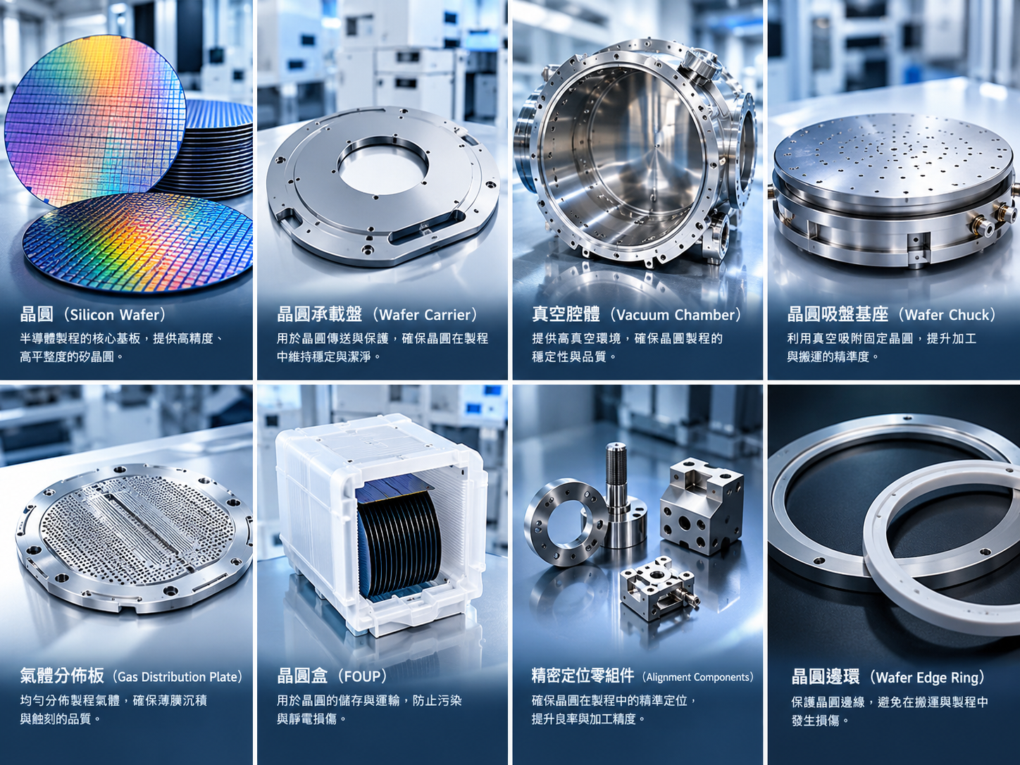
Wafer-related components, wafer precision machining (Precision Wafer & Semiconductor Equipment Machining), equipment and machinery, yield and CNC precision machining
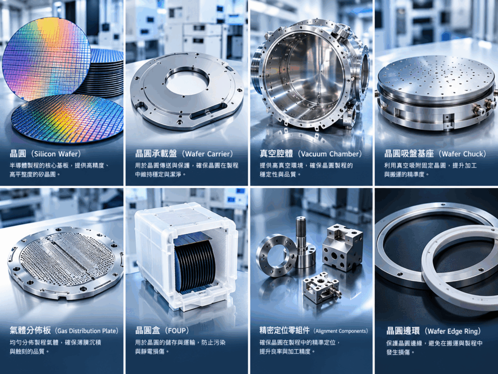
Precision Wafer Machining & Semiconductor Equipment Components
Precision Wafer & Semiconductor Equipment Machining is not limited to machining the wafer itself. It encompasses a broader range of manufacturing technologies, including wafer processing equipment, wafer handling systems, vacuum systems, gas delivery systems, process chambers, wafer support and positioning components, as well as various high-precision fixtures and mechanical components.
For semiconductor equipment suppliers, the purpose of precision CNC machining is to manufacture equipment components with high dimensional accuracy, flatness, parallelism, concentricity, surface cleanliness, and low-particle characteristics, thereby helping maintain wafer process stability and yield. Semiconductor manufacturing involves numerous process steps, making continuous metrology, inspection, and process control essential at critical stages.
1. What Does Precision Wafer Machining Include?
Wafer-related manufacturing can generally be divided into four major categories:
① Wafer & Substrate
- Silicon Wafer
- SOI Wafer
- SiC Wafer
- Glass / Quartz Substrate
- Compound Semiconductor Wafer
- 6-inch / 8-inch / 12-inch Wafer
② Wafer Handling & Supporting Components
- Wafer Carrier
- Wafer Cassette
- FOUP (Front Opening Unified Pod)
- End Effector
- Wafer Handling Arm
- Wafer Chuck
- Alignment Stage
- Wafer Lift Pin
- Wafer Support Ring
- Wafer Edge Ring
③ Semiconductor Process Equipment Components
- Vacuum Chamber
- Chamber Lid
- Chamber Base
- Gas Distribution Plate
- Showerhead
- Susceptor
- Electrode
- ESC / Electrostatic Chuck
- Gas Manifold
- Vacuum Manifold
- Slit Valve
- Flange
- Cooling Plate
④ Precision CNC Machined Components
- Precision Fixtures
- Positioning Bases
- Mounting Plates
- Base Plates
- Linear Guide Components
- Robot Arm Components
- Precision Shafts
- Fixtures
- Heat Sinks / Cooling Plates
- Micro-hole Components
Semiconductor equipment components are widely used in wafer handling, vacuum systems, gas delivery systems, and process chambers. Common materials include aluminum alloys, 316L stainless steel, and PEEK.
2. What Types of Wafer Processing Equipment Are Used?
The major equipment categories used in wafer manufacturing and semiconductor processing can be organized as follows:
| Equipment Type | Primary Function | Related CNC Components |
|---|---|---|
| Wafer Cleaning Equipment | Removal of particles and chemical contaminants | Chamber, Tank, Nozzle, Fixture |
| Lithography Equipment | Exposure and pattern transfer | Stage, Base, Chuck, Precision Mechanisms |
| Etching Equipment | Removal of thin-film materials | Chamber, Electrode, ESC, Gas Distribution Plate |
| Thin-Film Deposition Equipment | PVD / CVD / ALD processes | Vacuum Chamber, Showerhead, Susceptor |
| CMP Equipment | Chemical Mechanical Planarization | Carrier, Chuck, Plate, Fixture |
| Ion Implantation Equipment | Ion implantation into the wafer | Chamber, Beam Components, Fixture |
| Wafer Handling Equipment | Wafer transfer and handling | Robot Arm, End Effector, Aligner |
| Metrology Equipment | Dimensional, film-thickness, and process measurements | Stage, Mount, Fixture |
| Wafer Inspection Equipment | Defect detection and inspection | Chuck, Stage, Optical Mount |
| Packaging Equipment | Wafer-level and semiconductor packaging | Fixture, Carrier, Bonding Stage |
3. Key CNC Components for Precision Wafer & Semiconductor Equipment
3.1 Vacuum Chamber
The Vacuum Chamber is a critical component in semiconductor process equipment used for PVD, CVD, Etching, ALD, and other vacuum-based processes.
Key Requirements
- High-vacuum performance
- High leak tightness
- High flatness
- High flange dimensional accuracy
- Precise O-ring grooves
- CF / KF / ISO interfaces
- Low particle generation
- Low outgassing
- High internal surface cleanliness
Common Materials
Al 6061-T6, Al 6063, 316L Stainless Steel, 304 Stainless Steel, and specialty aluminum alloys
Typical CNC Machining Process
Rough Machining → Stress Relief → Semi-Finish Machining → Precision Finishing → Cleaning → Surface Treatment → Precision Inspection → Clean Packaging
4. Wafer Chuck
A Wafer Chuck is used to securely hold and stabilize a wafer during semiconductor processing, inspection, or handling.
Main Types
Vacuum Chuck
Uses vacuum suction to securely hold the wafer.
Electrostatic Chuck (ESC)
Uses electrostatic force to hold the wafer and is widely used in plasma etching and other semiconductor processes.
Mechanical Chuck
Uses mechanical clamping or positioning mechanisms to secure the wafer.
CNC Machining Considerations
- Flatness
- Parallelism
- Concentricity
- Vacuum holes
- Micro-holes
- Grooves
- Gas-flow channels
- Thermal-control structures
5. Gas Distribution Plate / Showerhead
The Gas Distribution Plate / Showerhead is a typical high-precision CNC-machined component used in semiconductor process equipment.
Its primary function is:
To distribute process gases uniformly across the wafer surface.
Therefore, machining is not simply a matter of drilling a large number of holes. It requires precise control of:
Hole Diameter + Hole Pitch + Hole Count + Hole Depth + Hole Geometry + Flatness + Surface Roughness + Gas-Flow Uniformity
Typical Materials
- Aluminum
- Aluminum Alloys
- 316L Stainless Steel
- Hastelloy
- Technical Ceramics
Possible Post-Processing
- Anodizing
- Electropolishing
- Cleaning
- Passivation
- Surface Treatment
Showerheads, gas distribution rings, and RF electrode mounts are representative process-chamber components that require precision manufacturing and CNC machining.
6. Wafer Handling Components
Because wafers must be transferred automatically throughout semiconductor manufacturing, Wafer Handling Systems are essential for safe and precise wafer transportation.
Main Components
End Effector
The component mounted at the end of a robotic arm for wafer handling and transfer.
Robot Arm
Transfers wafers between different process modules and equipment.
Wafer Aligner
Adjusts wafer orientation and position before processing or transfer.
Lift Pin
Raises and lowers the wafer during processing and transfer operations.
Wafer Carrier
Supports, stores, and transports wafers.
Key Requirements
These components typically require:
- Lightweight design
- High rigidity
- Low vibration
- High positioning accuracy
- Low particle generation
- High surface cleanliness
7. CNC Machining Process for Semiconductor Equipment Components
A typical manufacturing workflow can be structured as follows:
Customer Drawing / 3D CAD Data
↓
DFM / Manufacturing Process Evaluation
↓
Material Verification
↓
CNC Rough Machining
↓
Stress Relief
↓
5-Axis / 3+2 Precision Machining
↓
Micro-hole / Deep-hole Machining
↓
Precision Finishing
↓
Deburring
↓
Surface Treatment
↓
Ultrasonic Cleaning
↓
Precision Inspection
↓
Particle / Cleanliness Control
↓
Vacuum Packaging / Clean Packaging
↓
Final Inspection & Shipment
8. CNC Machine Tools for Wafer Equipment Components
① 3-Axis CNC Machining Center
Suitable for:
- Base Plates
- Fixtures
- Mounting Plates
- Structural Components
- General Chamber Components
② 4-Axis CNC Machining
Suitable for:
- Circular hole patterns
- Flanges
- Rings
- Cylindrical components
- Multi-sided machining
③ 5-Axis CNC Machining
5-Axis CNC machining is particularly valuable for complex semiconductor equipment components.
Suitable for:
- Complex curved surfaces
- Gas Distribution Components
- Robot Arms
- Chamber Components
- Impellers
- Precision Fixtures
- Multi-angle holes
5-axis machining can reduce positioning errors caused by repeated setups and improve machining consistency for complex components.
9. Micro-Hole Machining Equipment
Semiconductor equipment components frequently contain micro-hole structures and high-density hole patterns.
Possible technologies include:
- High-Speed CNC Machining
- Micro Milling
- Micro Drilling
- EDM (Electrical Discharge Machining)
- Wire EDM
- Laser Processing
This is particularly important for:
Gas Distribution Plates / Showerheads
These components may require a large number of precisely positioned micro-holes. Therefore, machining must control hole diameter, positional accuracy, hole depth, hole geometry, and internal surface quality.
10. Materials for Semiconductor Equipment CNC Machining
| Material | Typical Applications |
|---|---|
| Al 6061-T6 | Chamber, Base, Fixture |
| Al 6063 | Structural and Chamber Components |
| Al 7075 | High-Strength Mechanical Components |
| MIC-6 / Cast Aluminum | High-Flatness Base Plates |
| SUS304 / 304 Stainless Steel | General Vacuum Components |
| SUS316 / 316L Stainless Steel | Vacuum and Corrosive Environments |
| PEEK | Insulating and High-Temperature Components |
| POM | Mechanical Components and Fixtures |
| Quartz | Semiconductor Process Components |
| Alumina | Insulation and High-Temperature Components |
| SiC / Silicon Carbide | High-Temperature and Wear-Resistant Applications |
| AlN / Aluminum Nitride | Thermal Management and Ceramic Components |
11. Critical Precision Requirements for Semiconductor Equipment CNC Machining
For semiconductor equipment components, dimensional tolerance alone is not sufficient.
The following characteristics are also critical:
Dimensional Accuracy
Dimensional Accuracy
Flatness
Flatness
Parallelism
Parallelism
Perpendicularity
Perpendicularity
Concentricity
Concentricity
Coaxiality
Coaxiality
Position Accuracy
Position Tolerance
Surface Roughness
Surface Roughness
Vacuum Tightness
Vacuum Leak Tightness
Particle Control
Particle Control
Surface Cleanliness
Surface Cleanliness
Therefore, precision CNC machining for semiconductor applications can be understood as:
Dimensional Accuracy × Geometric Accuracy × Surface Quality × Cleanliness × Material Characteristics × Process Stability
12. What Is Wafer Yield?
In the semiconductor industry, Yield generally refers to the percentage of functional or conforming products obtained from the total production quantity.
The basic formula is:
Yield = Good Dies ÷ Total Dies × 100%
For example, if 96 out of 100 dies meet the required specifications:
Yield = 96 ÷ 100 × 100% = 96%
However, wafer yield is not determined by CNC components alone.
It can be affected by factors such as:
- Particle Contamination
- Chemical Contamination
- Overlay
- Critical Dimension (CD)
- Film Thickness
- Process Uniformity
- Etch Rate
- Temperature
- Pressure
- Gas Flow
- Equipment Stability
- Wafer Defects
Metrology and inspection systems are therefore used to monitor critical process parameters and provide feedback for process control.
13. Why Can CNC Components Affect Wafer Yield?
This is one of the most important technical topics when discussing semiconductor equipment components.
Poor Vacuum Chamber Machining
Potential chain:
Leak → Vacuum Instability → Process Variation → Wafer Defect → Yield Reduction
Non-Uniform Gas Distribution Plate
Potential chain:
Non-Uniform Gas Flow → Plasma / Deposition Non-Uniformity → Film Thickness Variation
Insufficient Wafer Chuck Flatness
Potential chain:
Wafer Positioning Variation → Process Variation → Device Performance Variation
Insufficient Wafer Handling Arm Accuracy
Potential chain:
Wafer Alignment Error → Handling Failure → Wafer Edge Damage / Particle Generation
Therefore:
CNC machining accuracy does not simply determine component dimensions. It can also contribute to the stability, repeatability, and contamination control of the semiconductor manufacturing process.
This is why semiconductor equipment manufacturers place strong emphasis on component consistency, precision, cleanliness, and process control.
14. Metrology & Inspection Equipment for Semiconductor CNC Components
After precision machining, components require comprehensive dimensional and surface inspection.
CMM — Coordinate Measuring Machine
Used to measure:
- Dimensions
- Position Tolerance
- Concentricity
- Parallelism
- Perpendicularity
Optical Measurement System
Suitable for:
- Micro dimensions
- Edges
- Profiles
- Contours
Surface Roughness Tester
Used to measure:
Ra / Rz / Surface Profile
Height Gauge
Used for:
- Height
- Step dimensions
- Flatness-related inspection
Roundness / Cylindricity Tester
Used to measure:
- Roundness
- Cylindricity
Interferometer
Can be used for high-precision measurement of:
- Surface flatness
- Surface profile
- Wafer topography
Advanced wafer metrology may also evaluate parameters such as flatness, thickness, stress, bow, warp, SORI, and nanotopography.
15. From Wafer Manufacturing to Precision CNC Components
The overall semiconductor manufacturing ecosystem can be represented as:
Silicon / SiC Wafer
↓
Wafer Manufacturing
↓
Cleaning / Lithography / Deposition / Etching / CMP
↓
Wafer Processing Equipment
↓
Vacuum Chamber
Gas Distribution Plate
Wafer Chuck
ESC
Susceptor
Wafer Carrier
Robot Arm
End Effector
Alignment Stage
↓
Precision CNC Machining
↓
Surface Treatment
↓
Cleaning
↓
Inspection / Metrology
↓
Clean Packaging
↓
Semiconductor Equipment Assembly
↓
Wafer Processing
↓
Yield / Process Stability
16. Recommended CNC Semiconductor Component Categories
For a semiconductor CNC machining manufacturer website, the product structure can be organized as follows:
A. Wafer Handling Components
- Wafer Carrier
- End Effector
- Robot Arm
- Wafer Aligner
- Lift Pin
B. Vacuum Components
- Vacuum Chamber
- Chamber Lid
- Vacuum Flange
- Vacuum Manifold
- Valve Components
C. Wafer Processing Components
- Wafer Chuck
- ESC / Electrostatic Chuck
- Susceptor
- Edge Ring
- Clamp Ring
- Electrode
D. Gas Distribution Components
- Gas Distribution Plate
- Showerhead
- Gas Ring
- Gas Manifold
- Flow Distribution Block
E. Precision CNC Components
- Base Plate
- Mounting Plate
- Precision Fixture
- Precision Stage
- Precision Shaft
- Micro-hole Components
F. Materials
Aluminum | SUS316L | SUS304 | PEEK | Quartz | Ceramic | SiC | AlN
Precision Semiconductor CNC Machining
For a professional semiconductor equipment manufacturing website, the overall positioning can be expressed as:
Precision CNC machining for wafer and semiconductor equipment components, covering wafer handling systems, vacuum chambers, gas distribution components, wafer chucks, process fixtures, and precision mechanical components. Our capabilities include 3-axis, 4-axis, and 5-axis CNC machining, micro-hole machining, surface treatment, precision inspection, cleaning, and clean packaging for semiconductor equipment applications.
Recommended SEO Keywords
Precision Wafer Machining
Wafer Components
Wafer Equipment Components
Semiconductor Equipment Components
Semiconductor CNC Machining
Semiconductor Parts Machining
Wafer Handling Components
Wafer Chuck
Vacuum Chamber Machining
Gas Distribution Plate
Showerhead
Electrostatic Chuck
Precision Semiconductor Components
5-Axis CNC Machining
Micro-Hole Machining
Core Positioning
Yung-Yi Technology’s Brand and Technology Positioning on its Website
“From wafer handling, vacuum chambers, gas distribution, wafer adsorption to process fixtures, we provide high-precision CNC machining, 5-axis machining, surface treatment, cleanroom cleaning, and precision measurement for semiconductor equipment components, assisting equipment manufacturers in improving process stability and yield.”
#Wafer Equipment Components #Semiconductor Equipment Components #Wafer Components #Semiconductor Parts Machining #Precision Wafer Machining #Wafer Carrier #Vacuum Chamber Machining #Wafer Chuck / Electrostatic Chuck #Wafer Handling Components #Semiconductor CNC Machining
#晶圓設備零組件 #半導體設備零組件 #晶圓零組件 #半導體零件加工 #晶圓精密加工 #晶圓載具 #真空腔體加工 #晶圓吸盤/靜電卡盤 #晶圓搬運零組件 #半導體 CNC 加工
Yongyi Technology Co., Ltd.

location_on 42756 No. 188-9, Section 1, Dafeng Road, Tanzi District, Taichung City, Taiwan
email yongyi-sales@umail.hinet.net
email justinwu6767@gmail.com